Graphite Solutions for Semiconductor and Ion Source Applications

Hongfeng Carbon Solutions provides advanced precision machining of high-purity graphite materials for ion-implantation, ion source grids, CVD, etching, electron beam evaporation components, and more. We also produce ultra-pure (<5ppm) VitreSeal™ vitreous impregnated graphite in-house to provide the value of an integrated supply chain.
Request a Quote

High-Purity Graphite Solutions for the Semiconductor Industry

Hongfeng Carbon Solutions has decades of experience processing ultra high-purity graphite materials for the semiconductor industry. We provide the highest quality graphite components for ion-implantation, ion source grids, etching, electron beam evaporation, crucibles, furnaces, chemical vapor deposition (CVD), and more.

We offer a wide range of premium isostatic graphite materials including POCO and are certified to further process POCO graphite materials for semiconductor applications.

Hongfeng Carbon Solutions produces our own ultra-pure (<5ppm) VitreSeal™ vitreous impregnated graphite materials. Our integrated supply chain and high production capacity enables us to provide the best value for the specialized components used in semiconductor equipment.

Isostatic Graphite Materials:
POCO Semiconductor Graphite Grades
• Others including Mersen, Toyo Tanso, and more.

Specialty Enhancements:
• Hongfeng PuriForge™ Purification process to <5ppm
• Hongfeng VitreSeal™ Vitreous Graphite Impregnation
•‍ Hongfeng PyroShield™ PyC Coating
•‍ Hongfeng SiCera™ Barrier SiC Coating
Request More Information
Cleanroom for semiconductor graphite - 03

How Graphite is Optimized for the Semiconductor Industry

01

Ultra High-Purity
Hongfeng Carbon Solutions can purify graphite through our PuriForge™ process, and we produce ultra-pure (<5ppm) VitreSeal™ material in-house. We operate a 10k-level clean room environment for processes, cleaning, and packaging the graphite parts we produce.

02

Thermal Stability
The excellent thermal properties of graphite allow it to uniformly conduct and dissipate heat for efficient and consistent etching. It can withstand extreme high temperatures required by many of the semiconductor processes. CrystiBarrier™ coatings can also enhance these properties.

03

Electrical Conductivity
Graphite's ideal electrical properties allow precise control of ion beams during the ion implantation process. This is critical for the performance of the semiconductor components.

04

Chemical Stability
The chemical stability of graphite prevents reactions that guarantee purity of the ion implantation process. It also resists chemical corrosion during the etching process. PyroSheild™ and CrystiBarrier™ coatings can also enhance these properties.

05

Uniform Properties
The premium isostatic graphite such as POCO and processing treatments offered by Hongfeng Carbon Solutions guarantee the components we produce have efficient, long-life operation.

06

VitreSeal™ Vitreous Graphite
Hongfeng Carbon Solutions' VitreSeal™ vitreous graphite material provides an optimized solution for critical ion beam applications by reducing contamination and particle emissions, and enhancing durability against beam erosion that increases component lifespan.
High-Purity Components for Ion Implantation
Ion Source Grids
VitreSeal™ Vitreous Graphite

Ultra-Pure Graphite for Semiconductor Processes

Quality Starts with Us!

In addition to using the highest quality graphite materials in the world, Hongfeng Carbon Solutions has over two decades of experience providing critical components for the semiconductor industry including ion-implantation, etching, chemical vapor deposition (CVD), and more.

Ion-beam technologies, such as ion implantation for semiconductor doping and ion source grids for particle acceleration, require materials that withstand high-energy ion bombardment while minimizing contamination, erosion, and particle release. Traditional high-purity graphite offers cost-effective thermal management, while enhancements like our VitreSeal™ vitreous impregnation reduce outgassing and particle emissions, and better resist beam erosion. Our PyroSheild™ PyC coating excels in low-sputtering coatings.

Cleanroom for Semiconductor Graphite Components

10k-level Clean Room
Ultrasonic Cleaning
Cleanroom for semiconductor graphite - 03
Cleanroom Packaging
Cleanroom for ultra-pure graphite
Semicon Graphite Processing
Learn More About our Materials

Ion-Implantation Parts

Graphite Tool for Semiconductor Applications by Hongfeng Carbon
Wafer Handling Components
Graphite Part for Ion Implantation 06
Ion Implanter Components
Graphite Part for Ion Implantation 04
Ion Implanter Parts
Source Assembly
See More of Our Ion-Implanter Parts

Ion Source Grids

Dished Ion Source Grids
Multi-layered Ion Source Grids
Ion Source Grids of All Shapes and Sizes
Extreme Precision at 0.012mm (12 microns)
See More of Our Ion Source Grids

Quality Materials & Quality Processes - It Starts With Us!

Graphite materials are critically important in semiconductor applications such as ion implantation, etching, chemical vapor deposition (CVD), electron beam evaporation, crucibles, and more. The use of ultra-pure graphite components is essential in these processes due to the superior thermal stability, high purity, and chemical resistance. These properties ensure precise and efficient processing, which is necessary to achieve optimal performance and reliability in semiconductor manufacturing.

Graphite materials are used in ion implantation for creating doped regions in semiconductors, where their purity and stability prevent contamination and ensure consistent results. In etching and CVD processes, graphite's thermal and chemical resistance allows for the precise deposition and removal of materials, essential for the intricate structures of semiconductor devices. For electron beam evaporation and the use of crucibles, graphite's high melting point and thermal conductivity enable efficient material vaporization and containment, ensuring high-quality thin films and wafers.

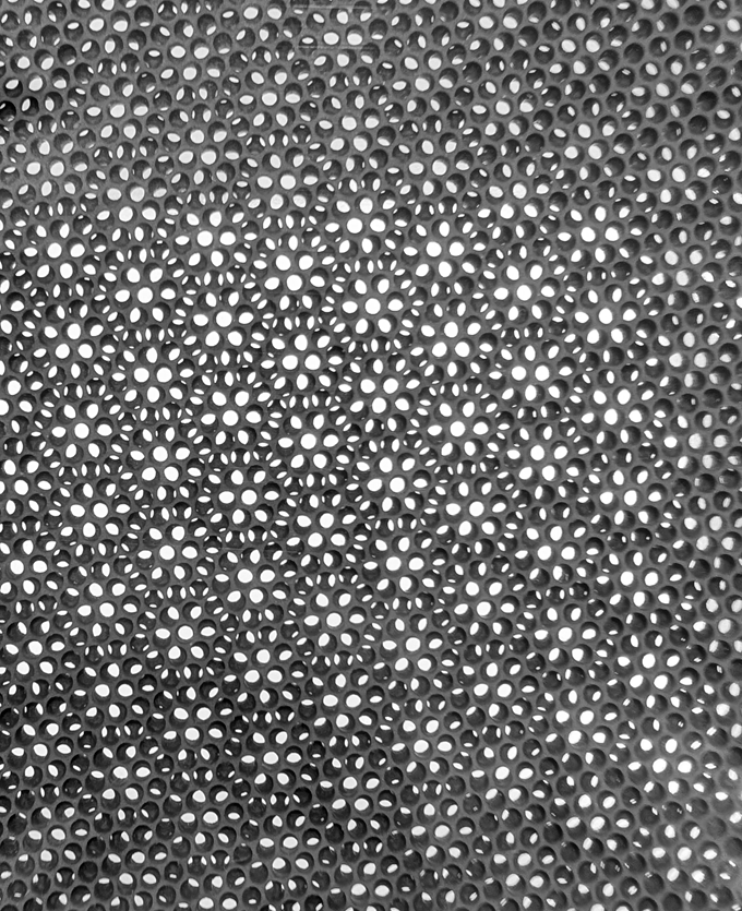
Hongfeng Carbon Solutions has developed a unique volcanic hardening process to create vitreous graphite materials that provide additional benefits in the semiconductor industry. Our VitreSeal™ material infuses high-purity graphite with vitreous (glassy) Carbon, a non-graphitizing amorphous Carbon, to seal pores and enhance surface properties. It is a highly specialized process that results in beamline components that virtually eliminate outgassing and particle emissions. They have exceptional purity and erosion resistance and are used in critical application spaces. The right graphite material ensures the reliability and longevity of the semiconductor equipment.

You can trust Hongfeng Carbon Solutions as your supplier for the graphite components used in the semiconductor manufacturing process. Our material development and advanced precision machining capabilities ensure that graphite components are produced with exact specifications, meeting the stringent requirements of the semiconductor industry. With over two decades of experience, we are experts and have developed innovative solutions to deliver high-quality graphite components tailored to your specific needs. Our commitment to quality, consistent delivery, and deep understanding of graphite applications in semiconductor manufacturing positions us as a leading innovator and reliable partner.

Optimizing Carbon Materials

Learn why we are trusted by clients around the world.
Why is Graphite better than Molybdenum or other metals in ion beam applications?
What is VitreSeal™ Vitreous Graphite?
What are advantages of POCO graphite?
What production capacity can Hongfeng Carbon Solutions provide?